- 您现在的位置:买卖IC网 > Sheet目录2000 > IDTSSTE32882KA1AKG (IDT, Integrated Device Technology Inc)IC REGISTERING CLK DRIVER 176BGA
1.25V/1.35V/1.5V REGISTERING CLOCK DRIVER WITH PARITY TEST AND QUAD CHIP SELECT
14
SSTE32882KA1
7314/8
THE INFORMATION IN THIS DOCUMENT IS SUBJECT TO CHANGE WITHOUT NOTICE
SSTE32882KA1
1.25V/1.35V/1.5V REGISTERING CLOCK DRIVER WITH PARITY TEST AND QUAD CHIP SELECT
COMMERCIAL TEMPERATURE RANGE
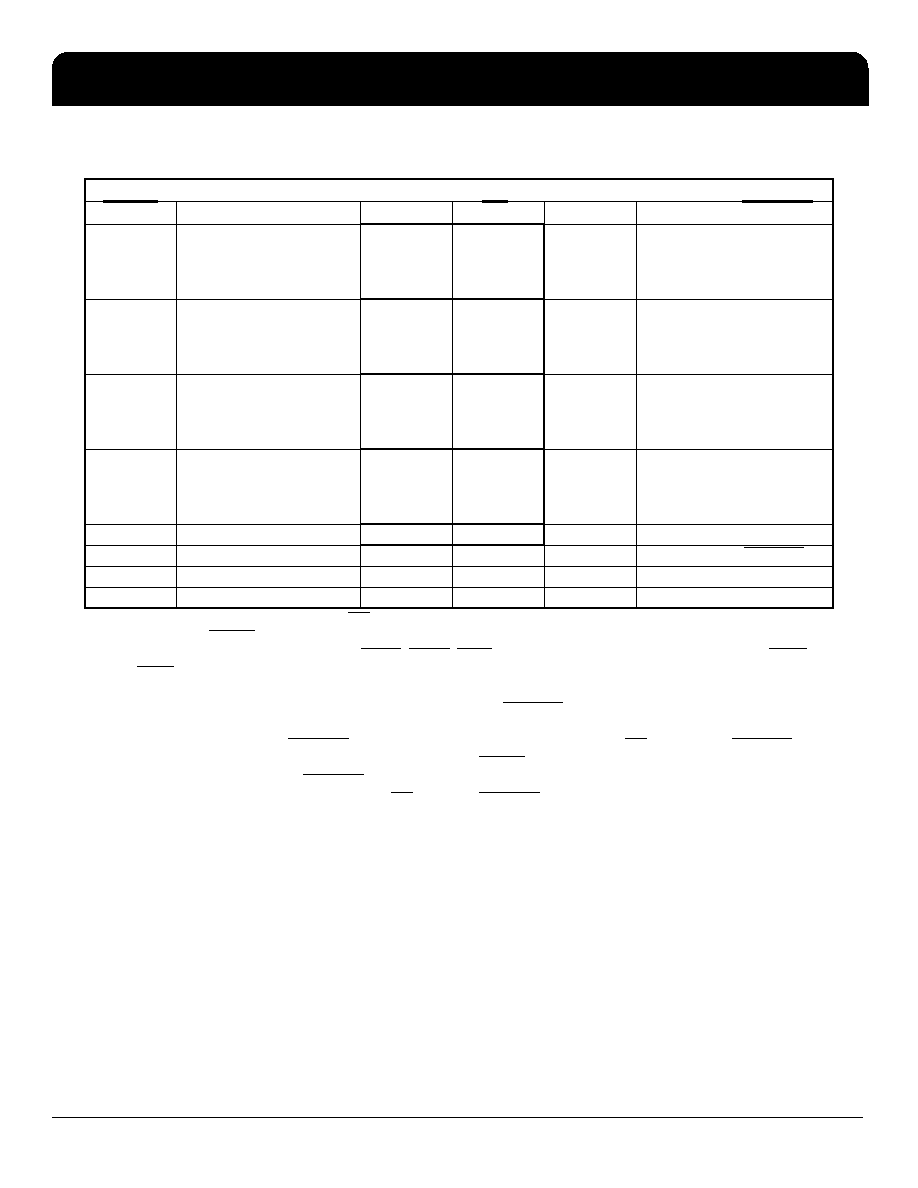
Parity, Low Power and Standby with QuadCS Mode Enabled
Inputs
Output
RESET
DCS[3:0]
CK1
1
It is illegal to hold both the CK and CK inputs at static logic high levels or static complementary logic levels (low
and high) when RESET is driven high.
CK1
Σ of A/C2
2
A/C = DA0..DA15, DBA0..DBA2, DRAS, DCAS, DWE. Inputs DCKE0, DCKE1, DODT0, DODT1, DCS0
and DCS1 are not included in this range. This column represents the sum of the number of A/C signals that are elec-
trically high.
PAR_IN3
3
PAR_IN arrivesone clock cycle afterdata to which it applies, ERROUT is issued three clock cycles after the fail-
ing data.
ERROUT4
4
This transition assumes ERROUT is high at the crossing of CK going high and CK going low. If ERROUT is
low, it stays latched low for exactly two clock cycles or until RESET is driven low.
HLXXX
XLXX
XXLX
XXXL
↑↓
Even
L
H
HLXXX
XLXX
XXLX
XXXL
↑↓
Odd
L
HLXXX
XLXX
XXLX
XXXL
↑↓
Even
H
L
HLXXX
XLXX
XXLX
XXXL
↑↓
Odd
H
HHHH
↑↓
XX
H5
5
Same three-cycle delay for ERROUT is valid for the de-select phase (see diagram)
H
XXXX
L or H
H or L
X
ERROUTn0
H
XXXX
L
X
H6
6
The system is not allowed to pull CK and CK low while ERROUT is asserted.
L
X or floating
X or floating X or floating X or floating X or floating
H
发布紧急采购,3分钟左右您将得到回复。
相关PDF资料
ISD1750SYR
IC VOICE REC/PLAY 50SEC 28-SOIC
ISD5008EYI
IC VOICE REC/PLAY 4-8MIN 28-TSOP
ISL12008IB8Z
IC RTC I2C LO-POWER 8-SOIC
ISL12020MIRZ-T7A
IC RTC/CALENDAR TEMP SNSR 20DFN
ISL12022IBZ-T7A
IC RTC/CALENDAR TEMP SNSR 8SOIC
ISL12022MAIBZ
IC RTC/CALENDAR TEMP SNSR 20SOIC
ISL12022MIBZ-T7A
IC RTC/CALENDAR TEMP SNSR 20SOIC
ISL12022MIBZR5421
IC RTC/CALENDAR TEMP SNSR 20SOIC
相关代理商/技术参数
IDTSSTE32882KA1AKG8
制造商:Integrated Device Technology Inc 功能描述:IC REGISTERING CLK DRIVER 176BGA
IDTSSTUB32866BHLF
功能描述:IC BUFFER 25BIT CONF REG 96LFBGA RoHS:是 类别:集成电路 (IC) >> 接口 - 专用 系列:- 特色产品:NXP - I2C Interface 标准包装:1 系列:- 应用:2 通道 I²C 多路复用器 接口:I²C,SM 总线 电源电压:2.3 V ~ 5.5 V 封装/外壳:16-TSSOP(0.173",4.40mm 宽) 供应商设备封装:16-TSSOP 包装:剪切带 (CT) 安装类型:表面贴装 产品目录页面:825 (CN2011-ZH PDF) 其它名称:568-1854-1
IDTSSTUB32S869AHLF
功能描述:IC REGISTERED BUFFER 150-TFBGA RoHS:是 类别:集成电路 (IC) >> 接口 - 信号缓冲器,中继器,分配器 系列:- 标准包装:160 系列:- 类型:转发器 Tx/Rx类型:以太网 延迟时间:- 电容 - 输入:- 电源电压:2.37 V ~ 2.63 V 电流 - 电源:60mA 安装类型:表面贴装 封装/外壳:64-TQFP 裸露焊盘 供应商设备封装:64-TQFP-EP(10x10) 包装:托盘 其它名称:Q5134101
IDTSSTUB32S869AHLFT
功能描述:IC REGISTERED BUFFER 150-TFBGA RoHS:是 类别:集成电路 (IC) >> 接口 - 信号缓冲器,中继器,分配器 系列:- 标准包装:160 系列:- 类型:转发器 Tx/Rx类型:以太网 延迟时间:- 电容 - 输入:- 电源电压:2.37 V ~ 2.63 V 电流 - 电源:60mA 安装类型:表面贴装 封装/外壳:64-TQFP 裸露焊盘 供应商设备封装:64-TQFP-EP(10x10) 包装:托盘 其它名称:Q5134101
IDTSSTVF16857AGLF
功能描述:IC DDR REGISTER 48-TSSOP RoHS:是 类别:集成电路 (IC) >> 接口 - 专用 系列:- 标准包装:3,000 系列:- 应用:PDA,便携式音频/视频,智能电话 接口:I²C,2 线串口 电源电压:1.65 V ~ 3.6 V 封装/外壳:24-WQFN 裸露焊盘 供应商设备封装:24-QFN 裸露焊盘(4x4) 包装:带卷 (TR) 安装类型:表面贴装 产品目录页面:1015 (CN2011-ZH PDF) 其它名称:296-25223-2
IDTSTAC9200X3NAEB1X
功能描述:IC AUDIO CODEC 2CH HD 32-QFN RoHS:是 类别:集成电路 (IC) >> 接口 - 编解码器 系列:- 标准包装:2,500 系列:- 类型:立体声音频 数据接口:串行 分辨率(位):18 b ADC / DAC 数量:2 / 2 三角积分调变:是 S/N 比,标准 ADC / DAC (db):81.5 / 88 动态范围,标准 ADC / DAC (db):82 / 87.5 电压 - 电源,模拟:2.6 V ~ 3.3 V 电压 - 电源,数字:1.7 V ~ 3.3 V 工作温度:-40°C ~ 85°C 安装类型:表面贴装 封装/外壳:48-WFQFN 裸露焊盘 供应商设备封装:48-TQFN-EP(7x7) 包装:带卷 (TR)
IDTSTAC9200X3NAEB1XR
功能描述:IC AUDIO CODEC 2CH HD 32-QFN RoHS:是 类别:集成电路 (IC) >> 接口 - 编解码器 系列:- 标准包装:2,500 系列:- 类型:立体声音频 数据接口:串行 分辨率(位):18 b ADC / DAC 数量:2 / 2 三角积分调变:是 S/N 比,标准 ADC / DAC (db):81.5 / 88 动态范围,标准 ADC / DAC (db):82 / 87.5 电压 - 电源,模拟:2.6 V ~ 3.3 V 电压 - 电源,数字:1.7 V ~ 3.3 V 工作温度:-40°C ~ 85°C 安装类型:表面贴装 封装/外壳:48-WFQFN 裸露焊盘 供应商设备封装:48-TQFN-EP(7x7) 包装:带卷 (TR)
IDTSTAC9200X3TAEB1X
功能描述:IC AUDIO CODEC 2CH HD 48-LQFP RoHS:是 类别:集成电路 (IC) >> 接口 - 编解码器 系列:- 标准包装:2,500 系列:- 类型:立体声音频 数据接口:串行 分辨率(位):18 b ADC / DAC 数量:2 / 2 三角积分调变:是 S/N 比,标准 ADC / DAC (db):81.5 / 88 动态范围,标准 ADC / DAC (db):82 / 87.5 电压 - 电源,模拟:2.6 V ~ 3.3 V 电压 - 电源,数字:1.7 V ~ 3.3 V 工作温度:-40°C ~ 85°C 安装类型:表面贴装 封装/外壳:48-WFQFN 裸露焊盘 供应商设备封装:48-TQFN-EP(7x7) 包装:带卷 (TR)